[Summary] PAGE: Processing-Using-DRAM Architecture-Circuits Co-Optimization for Efficient Acceleration of General Matrix-Vector Multiplication
Background
As large language models (LLMs) continue to grow in size and complexity, memory bandwidth and data movement have become major bottlenecks in AI system performance and energy efficiency. In particular, the decoding phase of LLM inference is often memory-bound, as general matrix-vector multiplication (GEMV) requires frequent access to large model weights stored in DRAM. Conventional computing architectures transfer these weights between memory and processing units, resulting in significant latency and energy overhead.
To address these challenges, processing-in-memory (PIM) and near-memory processing (NMP) architectures have been explored to reduce data movement. However, these approaches typically require additional processing units or substantial modifications to memory architectures, introducing area and implementation overhead.
Processing-Using-DRAM (PUD) offers an alternative by performing computations directly within existing DRAM peripheral circuits, particularly sense amplifiers (SAs). While previous PUD approaches have demonstrated Boolean logic operations, efficiently supporting multi-bit arithmetic and GEMV remains challenging due to limited computational parallelism and high operation latency.
Key Concept and Architecture
To overcome these limitations, SK hynix America and Cornell Tech jointly developed PAGE, a PUD architecture that accelerates GEMV operations through coordinated optimization of DRAM circuits and architecture. PAGE exploits existing DRAM computational capabilities while introducing minimal hardware modifications to improve parallelism, arithmetic efficiency, and data movement.
In the proposed architecture, compute-intensive operations such as general matrix multiplication (GEMM) and nonlinear functions remain on the host processor, while memory-intensive GEMV operations are offloaded to DRAM. By keeping model weights inside DRAM and transferring primarily input activations and output vectors, PAGE significantly reduces data movement between memory and the host processor.
PAGE introduces four key innovations:
- Mat-Level Parallelism: A modified hierarchical row decoder enables simultaneous activation of multiple DRAM mats, increasing computational parallelism and allowing configurable performance–power trade-offs.
- AP-Based Row Copy: An optimized row-copy mechanism reduces unnecessary sense amplifier operations, improving data movement efficiency within DRAM without modifying the underlying memory cells.
- Inversion-Enabled Sense Amplifier: A redesigned sense amplifier supports efficient in-place NOT operations, reducing the latency and energy overhead associated with multi-bit arithmetic while maintaining the transistor count of conventional sense amplifiers.
- Adaptive Adder-Tree Accumulation: An adaptive accumulation scheme dynamically adjusts the required arithmetic bit width, eliminating unnecessary computation cycles during multiply-and-accumulate operations.
Together, these optimizations enable efficient GEMV execution using DRAM peripheral circuits while preserving the fundamental DRAM storage structure.
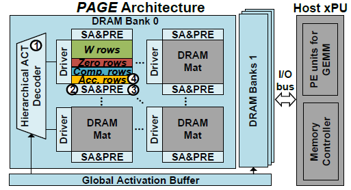
Figure 1. Overview of the PAGE architecture and its four key circuit and architecture-level optimizations for efficient GEMV acceleration.
Performance Evaluation
PAGE was evaluated through a combination of experimental validation, circuit-level simulation, and system-level performance analysis. The baseline PUD functionality was validated using a commercial SK hynix DRAM module integrated with an FPGA platform. The proposed circuit modifications were evaluated using TSMC 16nm technology, while a gem5-based in-house simulator was developed to analyze GEMV performance and energy consumption.
Experimental validation demonstrated correct PUD functionality across 1,000 tests, with less than 1.6% latency difference between DRAM measurements and the simulator. Circuit-level evaluation also confirmed that the proposed hierarchical decoder introduces only 1.4% area overhead compared with a conventional decoder.
System-level evaluations considered GEMV workloads with INT4 and INT8 precision across different matrix sizes. Without mat-level parallelism, PAGE achieved 3.9–5.5× lower end-to-end latency and 2.6–3.1× lower energy consumption compared with prior state-of-the-art PUD designs. By exploiting configurable mat-level parallelism, PAGE further improved performance, achieving up to 14.2× lower end-to-end latency.
These improvements demonstrate the combined benefits of reducing arithmetic operation overhead, increasing internal DRAM parallelism, and minimizing data movement between memory and processing units.

Figure 2. Comparison of GEMV execution latency and energy consumption between PAGE and prior PUD architectures across different matrix sizes and precisions.
Conclusion
PAGE demonstrates that DRAM can serve not only as a storage device but also as an efficient computational platform for memory-intensive AI workloads. Through architecture–circuit co-optimization, PAGE significantly improves GEMV performance and energy efficiency while requiring only limited modifications to conventional DRAM peripheral circuits.
This research highlights the potential of PUD as a practical approach to addressing memory bandwidth and data movement challenges in LLM inference. By extending the computational capabilities of DRAM without introducing dedicated processing units, PAGE provides a promising direction for developing more efficient and scalable AI memory systems.
DOI: https://dl.acm.org/doi/10.1145/3770743.3803970